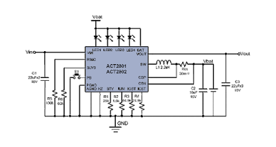
Power Bank Circuit Diagram
- Compact size of the power bank design and PCB: Smaller PCB leaves more room to use a larger battery, hence more energy rating of the power bank product. Smaller design leads to lower costs.
- Smaller system BOM: Helps improve reliability, as well as on the cost of the overall design.
- Integrated Safety features such as over-temperature, over-voltage protection.
- Scalable solution for different battery charging needs.
Active-Semi's ACT2813, ACT2802, and ACT2801 ICs offer the most compact system design for Power Banks. Power Bank systems can be implemented using a single Power Bank IC without the need for additional ICs such as an MCU or a protection IC. As such, ACT28xx based power bank solutions provide the smallest BOM, smallest PCB solutions available today.
ACT28xx Family integrates all the functions that a backup battery pack needs, including switching charger, boost converter and LED indication. ACT28xx also includes an input to obtain user feedback (for example, via a push button), to support various user-interface functions such as turn on/off charging and query charging status. The IC supports LED indication to display charging level on 4 LEDs.
Key Features & Benefits
- Dedicated Single Chip Solution for Mobile Power with Minimal Component Count
- High Charge & Discharge Efficiency, 96% Boost Efficiency (Vbat = 4.1V)
- <10 μA Low Battery Leakage Current in Hi-Z Mode during Storage
- Programmable Input Current Limit to up to 2A
- Programmable Constant Output Current in Boost Mode to up to 5V/2.4A
- No Load Shutdown and Push Button Turn-on
- Sophisticated Battery Protection for Over Current (OCP), Over Voltage (OVP), Over Temperature (OTP) and Short Circuit Protections (SCP). Battery Disconnection at Output Short
Below is the comparison of Active-Semi's ACT2081 EVK for Power Bank application (on the left) versus a PCB found in an off-the-shelf commercial product. The smaller PCB size and smaller component size enables smaller PCB design and associated costs. On the other hand, the smaller PCB can also enable the use of larger battery pack to store more energy within the power bank product.
Power Bank Block Diagram
Figure below shows the simplified implementation of power bank solution using ACT280x ICs. This supports 4 LEDs for battery charge status indication. Vin in connected to input voltage source which charges the battery attached to Vbat. The mobile device or tablet is connected to Vout to transfer charge either directly from Vin (while also charging battery at Vbat) or charge the mobile device with charge out of the battery (in the event Vin is not connected).
ACT280x EVK Block Diagram
Figure below is the block diagram for ACT28xx showing the architecture for charging the battery and providing system supply. The advantages of ACT28xx architecture and design versus the conventional one shown above are as follows.
- Requires minimum component count and PCB size
- High-efficiency, integrated solution with Boost, Buck, Battery charge management and LED indication
- Sophisticated battery protection for Over-temp, Over-voltages, Over-current and Short-circuit protection
Active-Semi's ACT28xx Architecture for Power Bank Applications
Figure below is the conventional architecture used in battery charging applications. This architecture typically has multiple ICs including MCU and battery power management ICs. Some of the disadvantages of this approach are as follows.
Low-efficiecncy in linear charger
Architecture results in larger PCB and solution size
Needs additional Battery protection board
Conventional architecture used in Power Bank Charger ICs
Evaluation Kits
Active-Semi has three Power Bank application evaluation kits including ACT2801, ACT2802, and ACT2813 ICs.
Source : active-semi.com


0 Comments:
Post a Comment